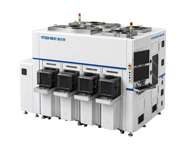
Product Overview
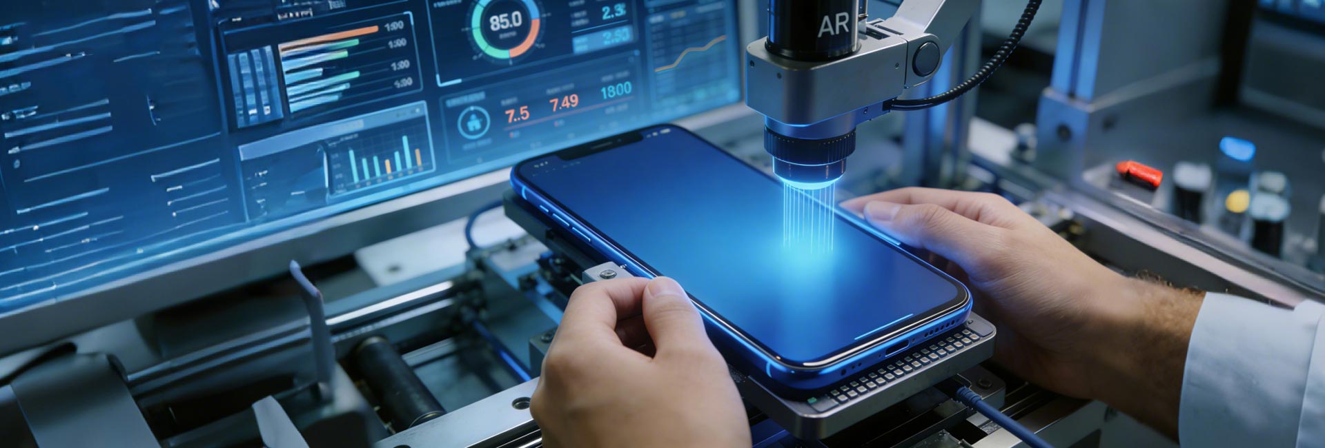
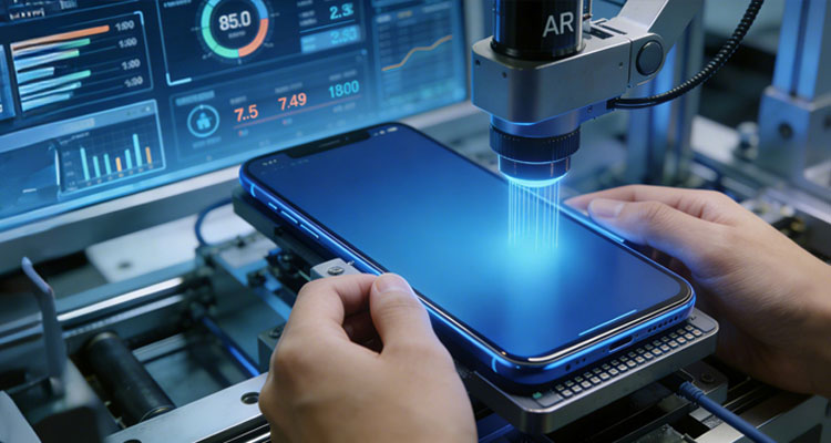
This equipment is mainly used for high-precision quality inspection of epitaxial wafer surfaces. By identifying and analyzing micron-level defects such as particles, contamination, and scratches, it can promptly detect surface anomalies that may affect subsequent processes and device performance, providing reliable support for product quality control and process optimization.
SiC epitaxial wafers is carried out throughout the entire process, from incoming materials and pretreatment to epitaxial growth, post-processing, and shipment. By deploying inspection at key process nodes, surface defects, contamination anomalies, and key process parameters are monitored throughout the entire process, ensuring stable and controllable product quality and improving the yield and consistency of epitaxial wafers.
SiC epitaxial wafers is carried out throughout the entire process, from incoming materials and pretreatment to epitaxial growth, post-processing, and shipment. By deploying inspection at key process nodes, surface defects, contamination anomalies, and key process parameters are monitored throughout the entire process, ensuring stable and controllable product quality and improving the yield and consistency of epitaxial wafers.
Product Advantages
-

- Wide field of view and high-precision detection
- Micron-level defects on the surface of SiC epitaxial wafers can be detected in a single scan.
-

- Customized lighting and precise imaging
- Achieve higher contrast imaging for typical defects such as particles, contamination, and scratches.
-

- Independent algorithm, reduced re-judgment
- Supports automatic defect identification and analysis, reducing the workload of manual re-judgment and microscopic confirmation.
-

- High efficiency and stability, covering the entire process
- Suitable for quality control of key processes such as incoming materials, pre-treatment, and before and after epitaxy.
Equipment Parameters
Parameters
Information and Data
Detection system
9K TDI camera
Cleanliness level
Class 100 cleanroom for the whole equipment
Detection software
Supports standard wafer inspection, inspection, stacking, statistics, and communication-based up-throw.
Pixel precision
1.4um
Minimum detection
4um
Equipment capacity
50WPH/6"; 25WPH/8"
Equipment size
L: 2200mm - W: 2200mm - H: 2200mm ( excluding electrical cabinet )
Applicable products
SiC substrate, substrate epitaxial wafer, patternless wafer
Testing items
Edge chipping and minor chipping, cracks on both sides, scratches on both sides, dirt and stains on both sides, dust on both sides, polycrystalline discoloration.
Other functions
OCR laser code recognition; Autofocus module
Process Application
Defect Display
-
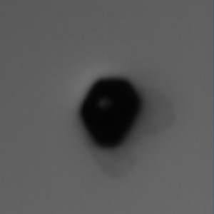
Hexagonal void
-

Internal cavity
-

Edge breakage
-

Scratch
-
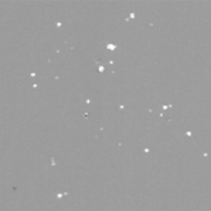
Particles