
Product Overview
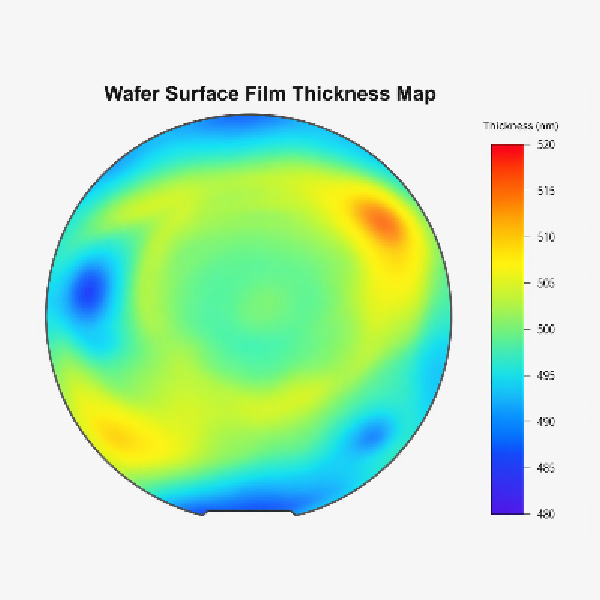
In the fabrication of optical waveguide devices, the uniformity and absolute thickness accuracy of the film thickness before etching are key factors determining the waveguide structure dimensions, etching depth control, and final optical performance. Optical waveguide pre-etching film thickness inspection equipment primarily addresses the quality inspection needs of waveguide layers, cladding, and related functional thin films before etching. It can perform high-precision measurement and analysis of film thickness, in-plane uniformity, local anomalies, edge thickness variations, and deposition defects, providing a reliable basis for subsequent etching process parameter setting and structural consistency control.
By implementing film thickness detection at key process nodes, risks such as etching deviation, mode mismatch, increased insertion loss, and decreased device consistency caused by film fluctuations can be effectively reduced, thereby improving product yield and end-product performance stability.
By implementing film thickness detection at key process nodes, risks such as etching deviation, mode mismatch, increased insertion loss, and decreased device consistency caused by film fluctuations can be effectively reduced, thereby improving product yield and end-product performance stability.
Product Advantages
-

- Non-contact high-precision measurement
- Avoids the risk of secondary contamination and surface damage to samples, meeting the high-precision thickness detection requirements of optical waveguide thin films.
-

- High - speed scanning and global assessment
- Supports rapid dot matrix sampling and in-plane thickness distribution reconstruction, enabling efficient analysis of thickness uniformity and local anomalies.
-

- Quick model changeover and process adaptation
- Supports rapid import of different product structures and process parameters, improving the efficiency of switching between multiple product models.
-

- Process improvement
- It can provide reliable data support for subsequent etching parameter setting, structural consistency control and yield optimization.
Equipment Parameters
Parameters
Information and Data
Detection system
Thickness sensor
Vertical resolution
0.01um
Repeatability
0.05um
Equipment capacity
60WPH/8" Wafer-30WPH/8" Wafer
Equipment size
L: 2500mm - W: 2500mm - H: 2200mm ( excluding electrical cabinet )
Applicable products
Transparent coating on wafer surface ( 3-50µm thickness )
Other functions
OCR laser code recognition; Autofocus module; TTV testing
Vertical resolution
0.01um
Repeatability
0.05um
Equipment capacity
60WPH/8" Wafer-30WPH/12" Wafer
Process Application
Defect Display