Product Overview
Glass wafers, as an important basic material for advanced packaging and optoelectronic integration, are widely used in key processes such as thinning substrates, temporary bonding substrates, optical waveguides, TGV glass interposers, and high-end optoelectronic packaging due to their high flatness, low dielectric loss, excellent optical transmittance, and good thermal stability.
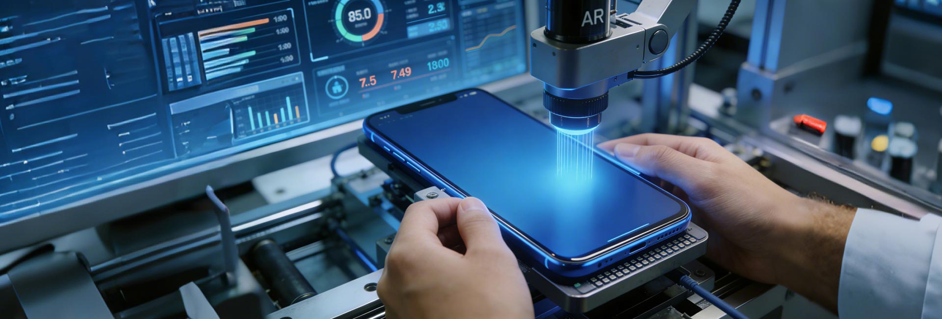
This equipment is mainly designed to meet the quality control needs of glass substrates during incoming materials, manufacturing processes, and final inspection. It can perform high-precision detection of scratches, cracks, edge chips, particles, contamination, bubbles, inclusions, coating abnormalities, and dimensional and appearance abnormalities. It enables full-process monitoring of the surface quality, edge condition, and process stability of glass wafers, thereby effectively reducing the risk of defects entering the product and improving product yield, consistency, and end-product reliability.
This equipment is mainly designed to meet the quality control needs of glass substrates during incoming materials, manufacturing processes, and final inspection. It can perform high-precision detection of scratches, cracks, edge chips, particles, contamination, bubbles, inclusions, coating abnormalities, and dimensional and appearance abnormalities. It enables full-process monitoring of the surface quality, edge condition, and process stability of glass wafers, thereby effectively reducing the risk of defects entering the product and improving product yield, consistency, and end-product reliability.
Product Advantages
-

- Large target area and high-precision imaging
- Micron-level defect detection can be completed in one scan, simplifying the operation process.
-

- Intelligent algorithms and efficient processing
- Supports rapid analysis of massive images, and can output mapping results without stitching the entire image.
-

- Multi -defect and multi-scenario compatibility
- It can detect scratches, cracks, chipping, particles, contamination, bubbles and coating abnormalities, and is compatible with various processes such as thinning substrates, optical waveguides, and TGV.
-

- Full-process quality control
- Covering key nodes such as incoming materials, pre-processing and shipment, reducing the risk of defects entering the product and improving product yield and consistency.
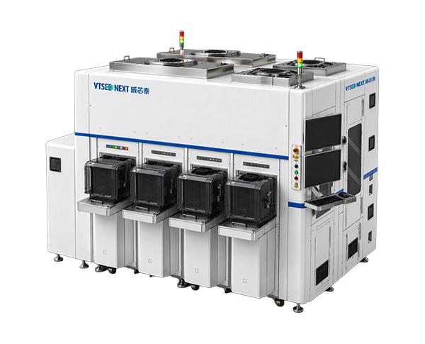
Equipment Parameters
Parameters
Information and Data
Detection system
TDI camera
Cleanliness level
Class 100 cleanroom for the whole equipment
Detection software
Supports standard wafer inspection, inspection, stacking, statistics, and communication-based up-throw.
Pixel precision
1.67µm/Pixel
Minimum detection
2.5um
Equipment capacity
28WPH/12" Wafer; 23WPH/310*310mm Panel
Equipment size
L: 2500mm - W: 2500mm - H: 2200mm ( excluding electrical cabinet )
Applicable products
Patternless glass wafers, 12" Wafer ( Notch )/ 310*310mm Panel, thickness 300-1500µm
Testing items
Particle, Scratch, Dig, Bubbles / Inclusion, Chips, Crack
Other functions
OCR laser code recognition; Autofocus module
Process Application
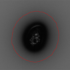
Defect Display
-
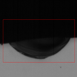
Edge breakage
-
Bubble
-
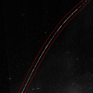
Scratch
-
Impurities
-
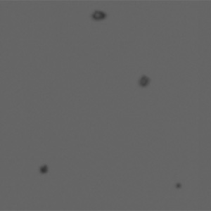
Particles